MIPS Microprocessor
a multicycle microprocessor and its assembler
Overview
My computing hardware course concluded with developing and testing the SystemVerilog description of a multicycle processor datapath. The processor runs a subset of the MIPS architecture. It was deployed on a Nexys A7 field programmable gate array (FPGA) evaluation board. Test programs were written in assembly and assembled by a Python script developed alongside the processor. The processor and assembler were developed collaboratively by a lab partner and me.
Design
Datapath
The design of the datapath began with developing the arithmetic logic unit (ALU). Our initial version of the ALU supported 7 instructions including ripple carry addition, logical and arithmetic shifting operations, and the logical operation bitwise AND. This version additionally included zero, equal, and overflow flags, as well as a reserved instruction code. Subsequent expansions of the ALU updated the adder to implement carry-lookahead addition, and added support for the logical operations OR, NOR, and XOR. Four, eight, and thirty-two to one multiplexers were developed alongside the operation logic to select the ALU’s output.
In the next phase of development we planned the execution flow of instructions. The datapath was to support 23 instructions including register and immediate input versions of ALU operations, load and save memory instructions, 2 branch instructions, and 3 jump instructions. Our plan for the states was guided by the separation of R, I, and J-type instructions in the MIPS architecture. We further divided the I-type instructions, giving separate state progressions to the memory instructions, immediate ALU operations, and the branch instructions. Alongside planning, we developed zero extension, sign extension, and ALU decode modules. These modules support preparation of operands for the ALU from their encoding in the instruction.
With the states planned, we developed the hardware to implement the execution flow. Each state corresponds to a cycle, and moves data between two registers of the datapath. Although this microprocessor is not pipelined, movement of data in the states is analogous to that of a five stage pipeline. The fetch and decode states retrieve instructions from memory and parse the bits of the instructions respectively. The third state of each instruction usually involves engaging the ALU, as in the execute stage of a five stage pipeline. The fourth and fifth states of the memory operations are used for memory access and data writing.
To facilitate completion of shorter instructions in less than 5 cycles, the datapath includes auxiliary pathways, and accomplishes multiple tasks during fetch and decode. During instruction fetch, the ALU is engaged to calculate the address of the next instruction in memory. During decode, the ALU is engaged to calculate the target address specified by branch and jump instructions. Using these early states for address calculation allows the microprocessor to determine the program counter (PC) by the third cycle. A description of dataflow in the states is provided in the table below.
| State | Objective |
|---|---|
| fetch | Fetch instruction from RAM |
| fetch | Calculate subsequent instruction address |
| decode | Decode instruction and retrieve register data |
| decode | Calculate PC relative address for control flow instructions |
| memAdr, Iexecute, execute | Execute ALU operation or calculate RAM address |
| brancheq, branchne | Resolve branch |
| jump, jumpal | Retrieve jump address from instruction |
| jumpreg | Retrieve jump address from the register file |
| jumpal | Write return address to the register file |
| memWrite, Iwriteback, ALUwriteback | Write ALU result to the register file |
| memRead | Read data from RAM |
| memWriteback | Write data to the register file |
Assembler
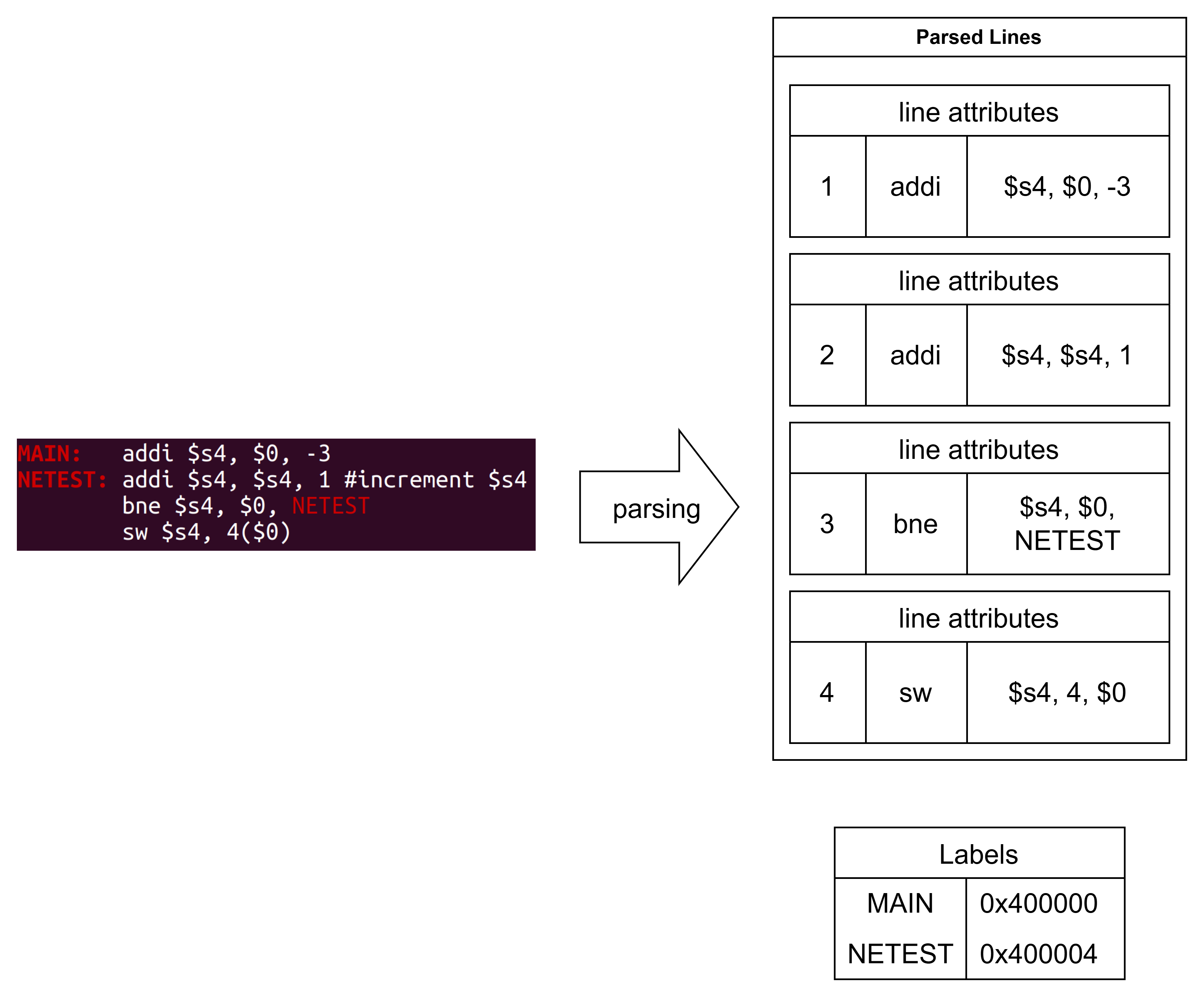
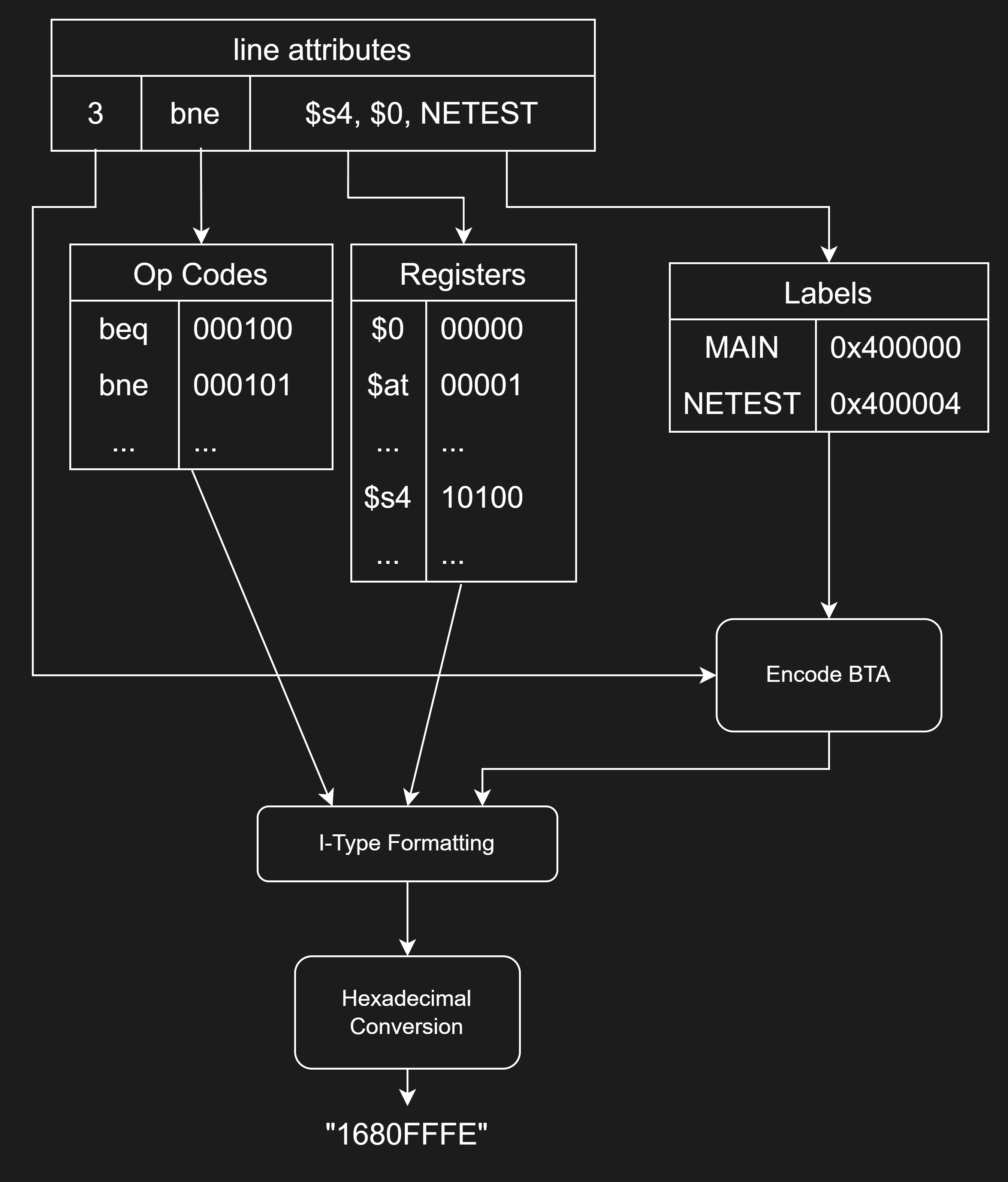
Our assembler accomplished conversion from MIPS assembly to hexadecimal machine words in two phases: parsing and assembling. The parsing phase produced two data structures from the input assembly program: a list of dictionaries describing the parsed lines, and a dictionary mapping labels in the program to their corresponding address. The assembling phase used these data structures with binary codes defined by the MIPS instruction set architecture (ISA) to build 32-bit machine words.
After reading the lines of an input assembly file, the parser handled comments and labels. Comments were identified discarded. Our datapath used a Von Neumann architecture with 32-bit instructions beginning at 0x400000 in memory, allowing us to calculate label addresses from their line number in the assembly file. These addresses were stored in the label dictionary before removing the labels.
The parser then passed through the assembly lines again to build the list of parsed lines. The parser scanned each line from left to right, gathering each line’s number, instruction, and arguments in a data structure.


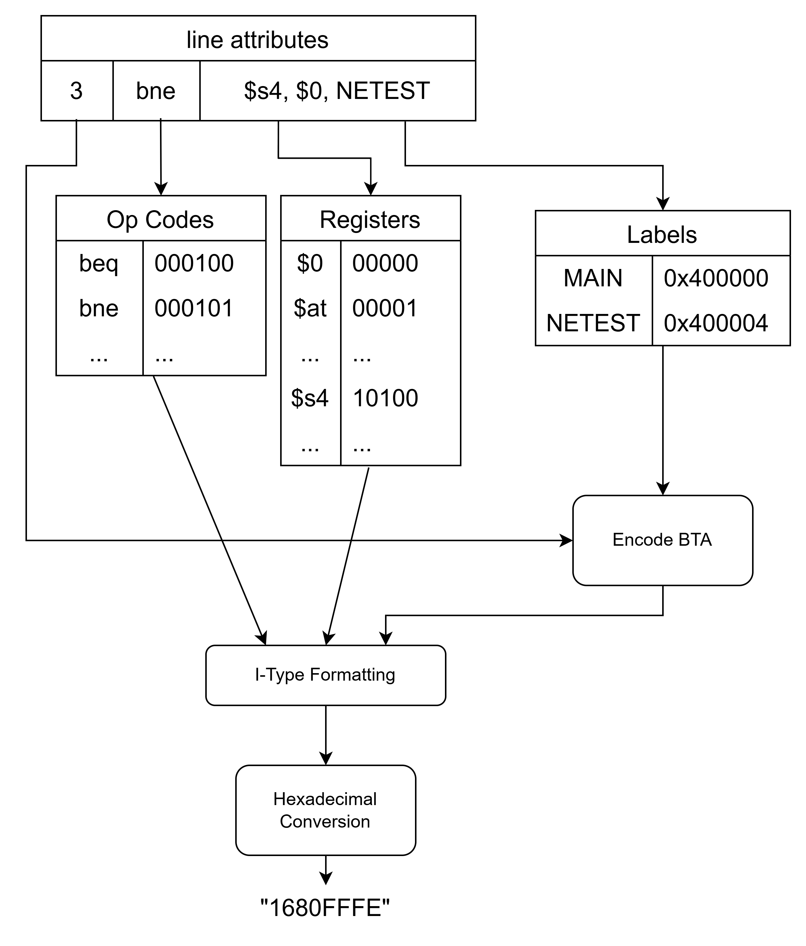
The assembler used the stored attributes of each line to build a machine word. It began by passing argument registers to a dictionary which maps register names to their ISA defined 5-bit codes. The encoding of the remaining portions of an instruction was dependent on its type. Our microprocessor’s supported R-Type instructions were stored in a list so that the assembler could identify them to be parsed separately. Since only two J-type instructions were supported, they were detected explicitly within the assembler’s logic. All other instructions were assembled as I-Type.

The MIPS ISA assigns all R-Type instructions the operation code 0, instead passing a function code to the ALU decoder. The instruction of a detected R-Type line was used to index a dictionary containing the supported function codes. The assembler’s logic also detected the three supported shift instructions, so that their shift amount could be converted to a 5-bit number.
I-type and J-type instruction assembling began with indexing a dictionary of operation codes with the instruction name. Branch instructions and J-Type instructions additionally indexed the label dictionary to find their target address. If an instruction was not detected as J-Type or a branch, it was assembled as an I-Type arithmetic or logic instruction. The lw and sw memory instructions fall under the arithmetic/logic designation, but were detected separately by the assembler since their immediate is the second argument instead of the third.
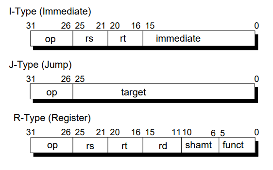
The assembling of all instructions concluded with ordering and concatenating the encoded binary values in the ISA defined format shown above. The 32-bit machine words were converted to hexadecimal for more compact display in an output memory file.


We verified the assembler through manual inspection of outputs covering the supported instructions.
Following assembler verification, initial tests of the datapath were carried out in the Vivado simulator. We wrote four tests programs covering the supported instructions. Following assembling, each of the programs was passed to Vivado as a memory initialization file. We verified the datapath’s operation by monitoring waveforms of the program counter, registers, control signals, operands, ALU output, and main memory.

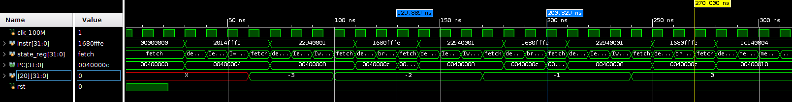
Debug functionalities, including a clock divider and debug ports, were provided in the assignment. The ports allowed us to view the contents of any register, or any of the first 256 words in data memory. Inspecting memory on the Nexys A7’s display allowed us to verify the implemented datapath’s test program execution.
References
1994
- IDT R30xx Family Software Reference Manual1994