Portal XR Inc. was founded by a group of students from Harvard and the University of Massachusetts Amherst with the vision of pushing the boundaries of extended reality (XR). The project seeks to improve the field of view of XR devices while maintaining a compact optical system. During my time working on the project, I designed a dual-axis MEMS mirror driver and controller to form the basis of the XR display system.
Design
Development of the display solution began with research into various display methods and trade studies weighing their attributes. Through this investigation it was determined that the XR display would use a laser projection system with a MEMS steering mirror. A further specified trade study into MEMS mirror types led to the selection of a two axis electromagnetic mirror to steer the display laser. Hardware design began with an analog driver for the MEMS mirror and proceeded to incorporate further interacting subsystems.
Projection hardware block diagram
Projection hardware block diagram
Projection hardware block diagram
Projection hardware block diagram
The selected mirror incorporated a linear slow axis and resonant fast axis, allowing the slow axis to be controlled according to nearly arbitrary waveforms within its bandwidth, and requiring that the fast axis be driven within a very narrow range of its resonant frequency. It followed that the primary goals of the mirror driver were
to produce current signals to actuate the two mirror axes
to isolate a back EMF signal which facilitates finding the fast axis resonant frequency
Arbitrary waveforms could be converted to current signals and sent to the slow axis by placing it in the feedback path of a noninverting amplifier. The fast axis could be driven by a square wave current signal generated by a current source feeding an H bridge, switched at the resonant frequency. The back EMF signal could be isolated from either the fast or slow axis coils. I chose to isolate it from the slow axis where it would be well separated from the low frequency signal driving the coil.
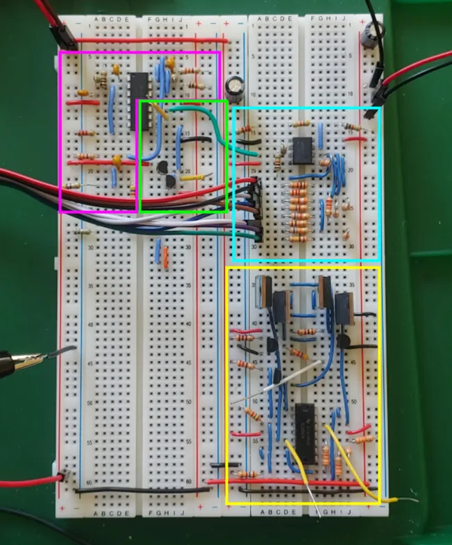
MEMS mirror driver breadboard test circuit with sections approximately marked: slow axis driver (green), fast axis driver (yellow), back EMF filter (magenta), and slow axis DAC (cyan).
MEMS mirror driver breadboard test circuit with sections approximately marked: slow axis driver (green), fast axis driver (yellow), back EMF filter (magenta), and slow axis DAC (cyan).
Preliminary testing of the mirror driver with a resistive test load verified its ability to generate appropriate current signals from 1Vpp waveforms in the slow axis and 5V control signals in the fast axis. Testing with the MEMS mirror revealed that the frequency resolution of the function generator producing fast axis control signals was insufficient for generating a signal near enough to the mirror’s resonance to actuate the fast axis or produce an observable back EMF signal. With this, work commenced on a more precise timing generator.
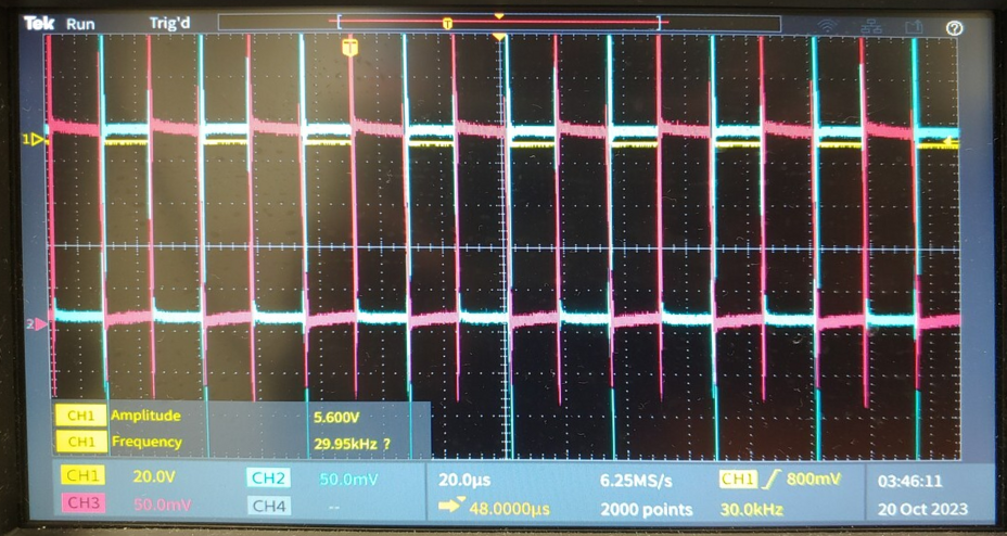
Fast axis driver resistive load test. Channel 1 shows the control input; channels 2 and 3 show the differential output.
Fast axis driver resistive load test. Channel 1 shows the control input; channels 2 and 3 show the differential output.
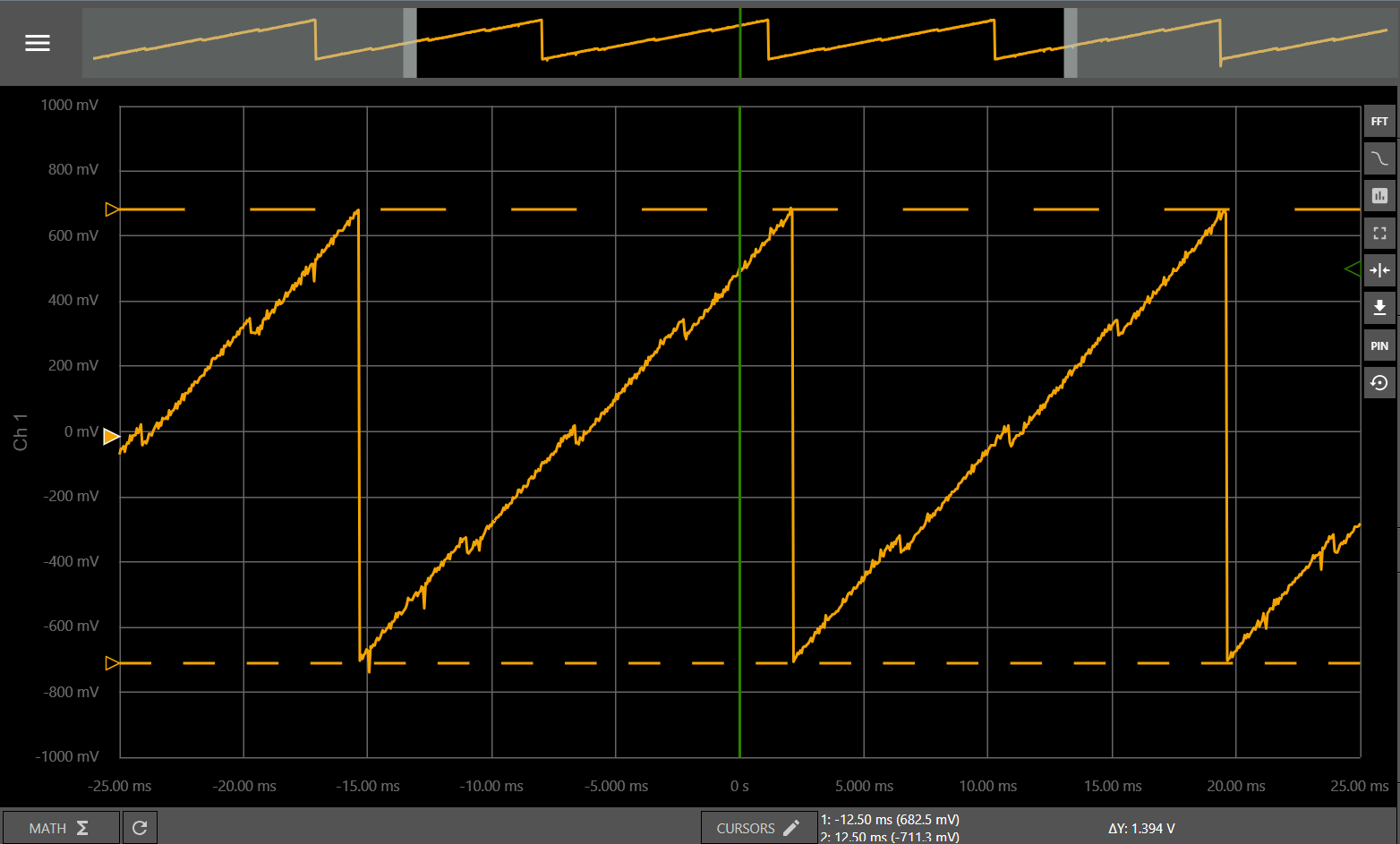
Slow DAC test with digital ramp wave input. Discontinuities during the ramp's rise are caused by error in weighting the second most significant bit.
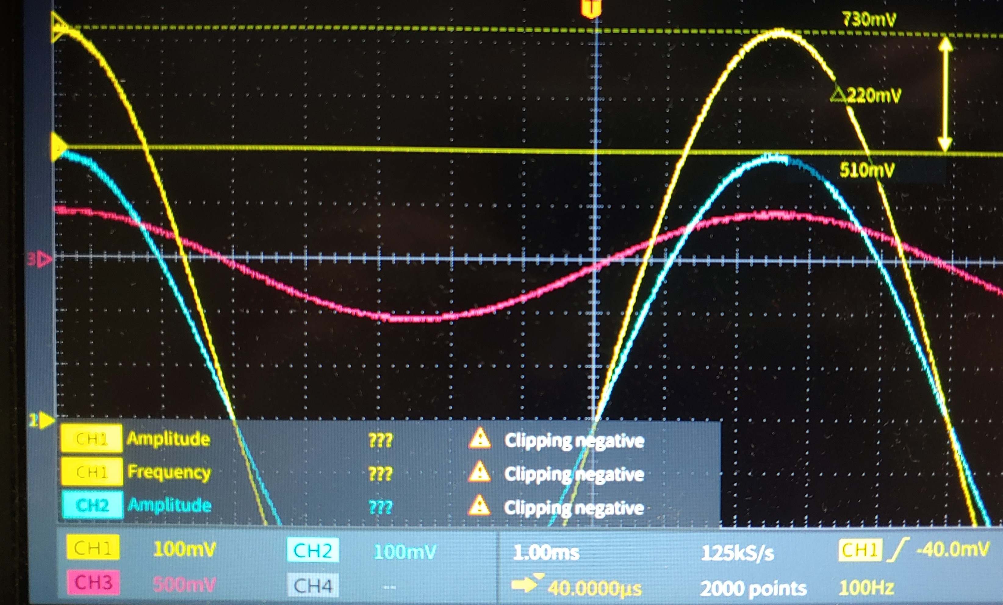
Slow axis driver resistive load test. In this test the DAC is bypassed and a sine wave drive signal is fed directly from a function generator. Channels 1 and 2 show the differential output; channel 3 shows the slow axis input. The circuit's gain was set such that a 1Vpp input produces a 220mV amplitude output across the test load—the maximum recommended by the MEMS mirror's datasheet.
Slow DAC test with digital ramp wave input. Discontinuities during the ramp's rise are caused by error in weighting the second most significant bit.
Slow axis driver resistive load test. In this test the DAC is bypassed and a sine wave drive signal is fed directly from a function generator. Channels 1 and 2 show the differential output; channel 3 shows the slow axis input. The circuit's gain was set such that a 1Vpp input produces a 220mV amplitude output across the test load—the maximum recommended by the MEMS mirror's datasheet.
The purpose of the timing generator is to synchronize the movements of the MEMS mirror axes with the laser. This was accomplished by a system of interrelated counters that generate mirror drive signals alongside signals to be sent to the memory and laser subsystems for retrieving pixel information. The timing generator additionally achieved greater frequency resolution by leveraging a 400MHz clock, which allowed a resolution of ~4Hz in the neighborhood of the mirror’s 30kHz nominal resonant frequency. The counters and surrounding logic were implemented in SystemVerilog and deployed on an Arty A7. For ease of interfacing, top level commands to reset the counters or update the fast axis drive frequency could be sent to an Arduino over serial which transferred the signals to the A7.
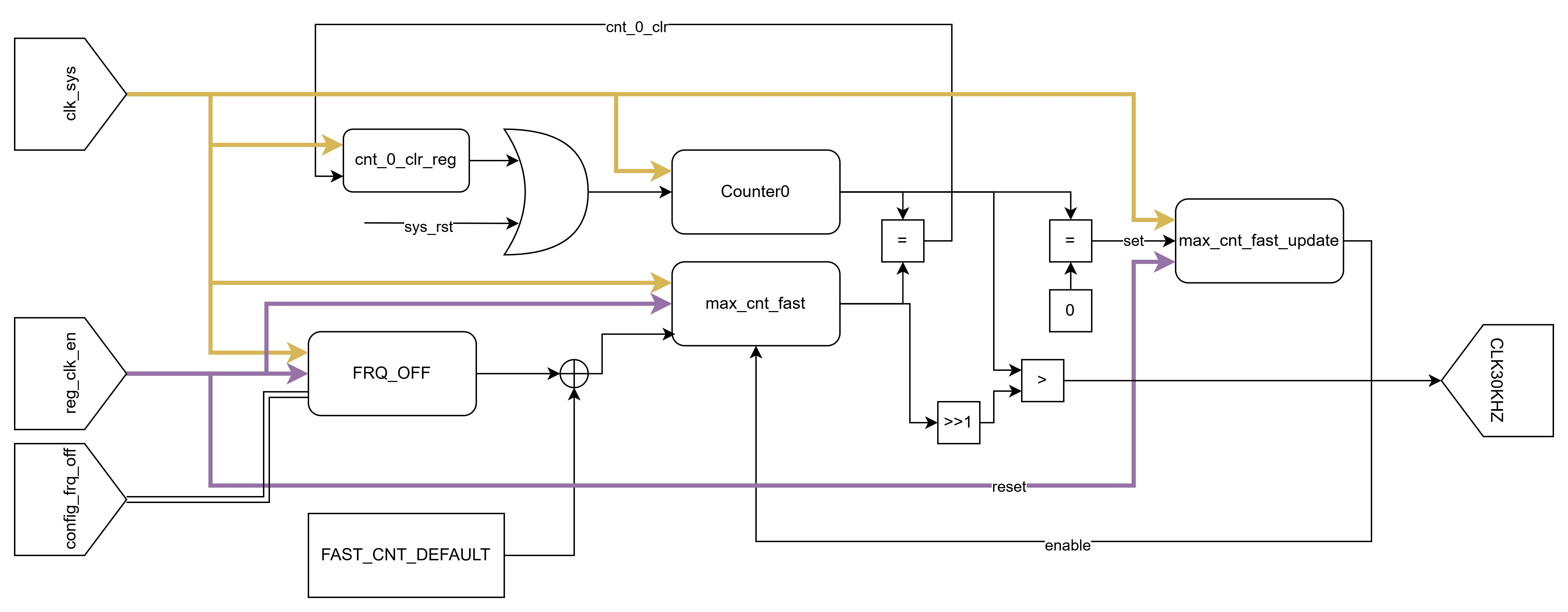
Fast axis architecture. The 'FAST_CNT_DEFAULT' parameter produces the fast axis' nominal 29.3kHz resonant frequency and is tuned further by a variable frequency offset. All registers are clocked to a fast 'clk_sys'. Registers associated with the frequency offset are enabled by a slower, synchronous, config register clock enable. 'FRQ_OFF' was implemented with a shift register input to reduce I/O usage.
Fast axis architecture. The 'FAST_CNT_DEFAULT' parameter produces the fast axis' nominal 29.3kHz resonant frequency and is tuned further by a variable frequency offset. All registers are clocked to a fast 'clk_sys'. Registers associated with the frequency offset are enabled by a slower, synchronous, config register clock enable. 'FRQ_OFF' was implemented with a shift register input to reduce I/O usage.
Fast axis architecture. The 'FAST_CNT_DEFAULT' parameter produces the fast axis' nominal 29.3kHz resonant frequency and is tuned further by a variable frequency offset. All registers are clocked to a fast 'clk_sys'. Registers associated with the frequency offset are enabled by a slower, synchronous, config register clock enable. 'FRQ_OFF' was implemented with a shift register input to reduce I/O usage.
Fast axis architecture. The 'FAST_CNT_DEFAULT' parameter produces the fast axis' nominal 29.3kHz resonant frequency and is tuned further by a variable frequency offset. All registers are clocked to a fast 'clk_sys'. Registers associated with the frequency offset are enabled by a slower, synchronous, config register clock enable. 'FRQ_OFF' was implemented with a shift register input to reduce I/O usage.
Raster scan diagram depicting the values of the fast and slow axis counters Q0 and Q1 in terms of the 'max_cnt_fast' register value, and parameters 'hblank' and 'vblank'. Blanking period lengths are set such to maintain an image's resolution alongside the necessary counts for running the fast and slow axes.
Raster scan diagram depicting the values of the fast and slow axis counters Q0 and Q1 in terms of the 'max_cnt_fast' register value, and parameters 'hblank' and 'vblank'. Blanking period lengths are set such to maintain an image's resolution alongside the necessary counts for running the fast and slow axes.
Raster scan diagram depicting the values of the fast and slow axis counters Q0 and Q1 in terms of the 'max_cnt_fast' register value, and parameters 'hblank' and 'vblank'. Blanking period lengths are set such to maintain an image's resolution alongside the necessary counts for running the fast and slow axes.
Raster scan diagram depicting the values of the fast and slow axis counters Q0 and Q1 in terms of the 'max_cnt_fast' register value, and parameters 'hblank' and 'vblank'. Blanking period lengths are set such to maintain an image's resolution alongside the necessary counts for running the fast and slow axes.
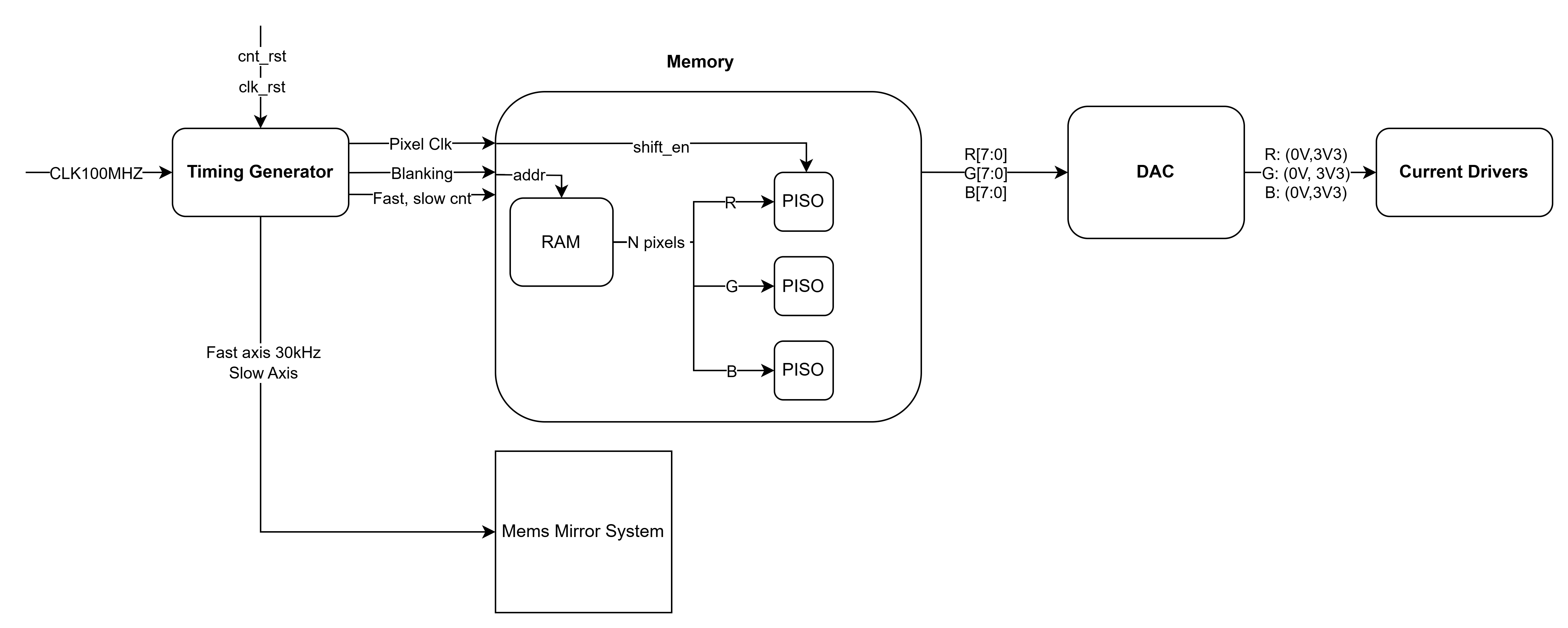
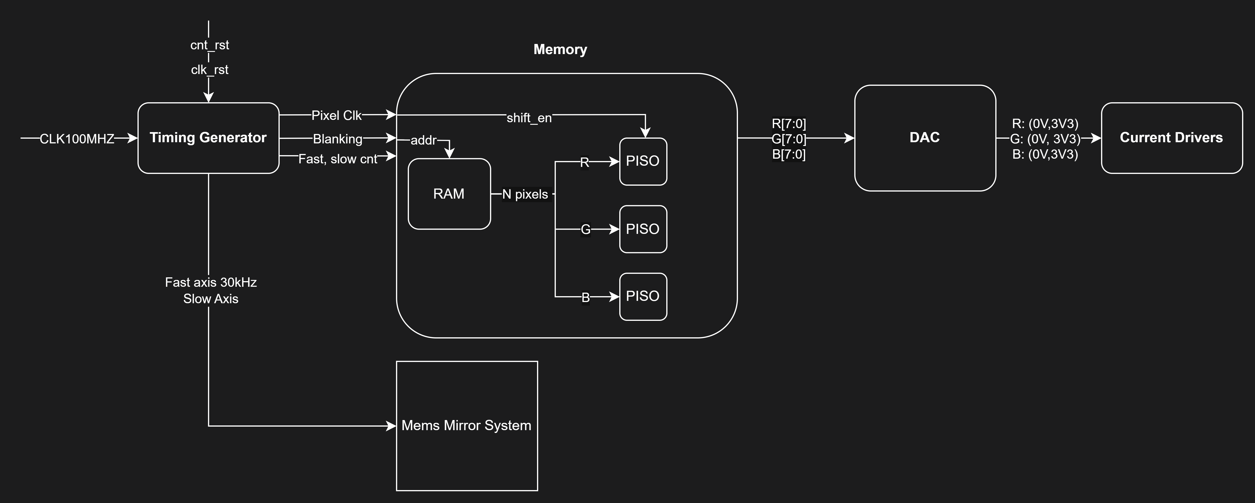
Memory system control signal generation architecture. Counter 3 is responsible for dividing the system clock into a pixel clock for images with a low horizontal resolution. Counter 4 counts pixels as they pass to retrieve the appropriate data from memory. Counter 5 is responsible for repeating lines in images with a low vertical resolution.
Memory system control signal generation architecture. Counter 3 is responsible for dividing the system clock into a pixel clock for images with a low horizontal resolution. Counter 4 counts pixels as they pass to retrieve the appropriate data from memory. Counter 5 is responsible for repeating lines in images with a low vertical resolution.
Memory system control signal generation architecture. Counter 3 is responsible for dividing the system clock into a pixel clock for images with a low horizontal resolution. Counter 4 counts pixels as they pass to retrieve the appropriate data from memory. Counter 5 is responsible for repeating lines in images with a low vertical resolution.
Memory system control signal generation architecture. Counter 3 is responsible for dividing the system clock into a pixel clock for images with a low horizontal resolution. Counter 4 counts pixels as they pass to retrieve the appropriate data from memory. Counter 5 is responsible for repeating lines in images with a low vertical resolution.
Tests of the timing generator verified sufficient frequency resolution for the appearance of a measurable back EMF signal, enabling actuation of the mirror’s fast axis. Successful single axis actuations were followed by a dual axis test.
Test projection setup with a red laser, dichroic filter, and the MEMS mirror housed on a 3D printed stand
Dual axis actuation test. The slow axis is activated first at 0:01. The fast axis is activated at 0:02 and the frequency offset is swept until resonance is reached at 0:13.
Test projection setup with a red laser, dichroic filter, and the MEMS mirror housed on a 3D printed stand
Following successful dual axis actuation, and in preparation for higher speed laser driver circuitry, the mirror driver was consolidated into a PCB. In addition to capturing the existing schematic, I updated the slow axis DAC and connectors to the MEMS mirror, and added coil inhibit signals. The original summing amplifier DAC showed significant error in conversion of the second most significant bit arising from approximation in the resistor ratios and 5% tolerances. This error not only affected mirror actuation, but injected a small erroneous signal into the back EMF filter’s bandwidth. The DAC was replaced with a SPI DAC IC to be driven from a MicroBlaze instantiated in the A7.
MEMS mirror driver PCB layout with sections approximately marked: slow axis driver (green), fast axis driver (yellow), back EMF filter (magenta), slow axis DAC (cyan), and coil inhibits (red).
Assembled MEMS mirror driver PCB. Connectors J1, J2, and J3 were positioned to interface with three of the Arty A7s four side connectors. J4a and J4b house the Arduino MKR Zero. J6 sends the two-axis drive signals to the mirror.
The first revision of the PCB houses the fast and slow axis drivers, back EMF filter and amplifier, slow axis DAC, and an Arduino MKR Zero, with connectors for the MEMS mirror and FPGA, as well as a pin header of signals exposed for debugging. It uses a four layer stack up composed of two signal layers, a ground plane, and a split, dual supply power plane.
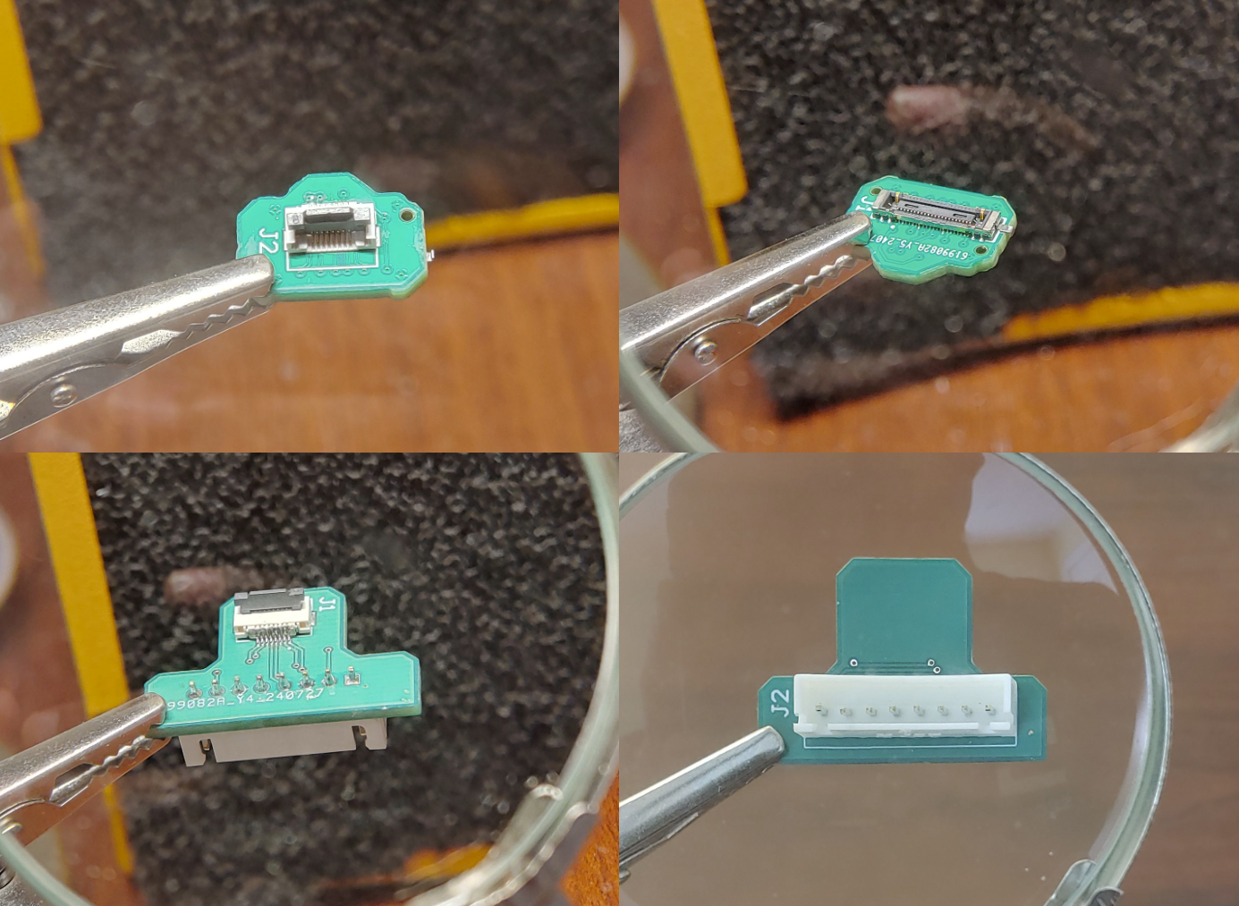
The original mirror connector was a flexible PCB with polyimide stiffener. Repeated flexing in stiffened regions eventually caused solder joint failures in 2 of 5 assembled connectors. The flex connector was replaced with two small, FR4 boards and a ribbon cable, offering greater strength to the mirror receptacle’s contacts and facilitating mating.
Flex connector replacement PCBs. The left images are top views showing the ribbon cable's connector. The right images are bottom views which mate with the MEMS mirror (upper right) and driver PCB (lower right).
Flex connector replacement PCBs. The left images are top views showing the ribbon cable's connector. The right images are bottom views which mate with the MEMS mirror (upper right) and driver PCB (lower right).


, fast axis driver (yellow), back EMF filter (magenta), and slow axis DAC (cyan)")


, fast axis driver (yellow), back EMF filter (magenta), slow axis DAC (cyan), and coil inhibits (red)")
-1400.webp "Assembled MEMS mirror driver PCB")
.jpg)